Author Affiliations
Abstract
1 Department of Electrical and Computer Engineering, University of Pittsburgh, Pittsburgh, PA 15261, United States of America
2 School of Optoelectronic Engineering and Instrument Science, Dalian University of Technology, Dalian 116081, People’s Republic of China
3 Westinghouse Electric Company LLC, Pittsburgh, PA 15235, United States of America
4 Nuclear Reactor Laboratory, Massachusetts Institute of Technology, 138 Albany Street, Cambridge, MA 02139, United States of America
The femtosecond laser has emerged as a powerful tool for micro- and nanoscale device fabrication. Through nonlinear ionization processes, nanometer-sized material modifications can be inscribed in transparent materials for device fabrication. This paper describes femtosecond precision inscription of nanograting in silica fiber cores to form both distributed and point fiber sensors for sensing applications in extreme environmental conditions. Through the use of scanning electron microscope imaging and laser processing optimization, high-temperature stable, Type II femtosecond laser modifications were continuously inscribed, point by point, with only an insertion loss at 1 dB m-1 or 0.001 dB per point sensor device. High-temperature performance of fiber sensors was tested at 1000 ℃, which showed a temperature fluctuation of ±5.5 ℃ over 5 days. The low laser-induced insertion loss in optical fibers enabled the fabrication of a 1.4 m, radiation-resilient distributed fiber sensor. The in-pile testing of the distributed fiber sensor further showed that fiber sensors can execute stable and distributed temperature measurements in extreme radiation environments. Overall, this paper demonstrates that femtosecond-laser-fabricated fiber sensors are suitable measurement devices for applications in extreme environments.
femtosecond laser manufacturing optical fiber sensor device fabrication extreme environment sensing International Journal of Extreme Manufacturing
2021, 3(2): 025401
Author Affiliations
Abstract
1 School of Sciences, Hebei University of Technology, Tianjin 300401, China
2 School of Physical Science and Technology, Southwest University, Chongqing 400715, China
3 Hebei Jiya Electronics Co., Ltd., Shijiazhuang 050071, China
4 Hebei Provincial Research Center of LCD Engineering Technology, Shijiazhuang 050071, China
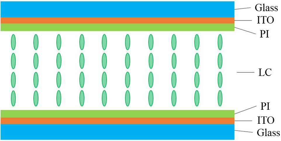
Image sticking in liquid crystal display (LCD) is related to the residual direct current (DC) voltage (RDCV) on the cell and the dynamic response of the liquid crystal materials. According to the capacitance change of the liquid crystal cell under the DC bias, the saturated RDCV (SRDCV) can be obtained. The response time can be obtained by testing the optical dynamic response of the liquid crystal cell, thereby evaluating the image sticking problem. Based on this, the image sticking of vertical aligned nematic (VAN) LCD (VAN-LCD) with different cell thicknesses (3.8 μm and 11.5 μm) and different concentrations of γ-Fe2O3 nanoparticles (0.017 wt.%, 0.034 wt.%, 0.051 wt.%, 0.068 wt.%, 0.136 wt.%, 0.204 wt.%, and 0.272 wt.%) was evaluated, and the effect of nano-doping was analyzed. It is found that the SRDCV and response time decrease firstly and then increase with the increase of the doping concentration of γ-Fe2O3 nanoparticles in the VAN cell. When the doping concentration is 0.034 wt.%, the γ-Fe2O3 nanoparticles can adsorb most of the free impurity ions in liquid crystal materials, resulting in 70% reduction in the SRDCV, 8.11% decrease in the decay time, and 15.49% reduction in the rise time. The results show that the doping of γ-Fe2O3 nanoparticles can effectively improve the image sticking of VAN-LCD and provide useful guidance for improving the display quality.
nanoparticles doping image sticking SRDCV response time VAN-LCD Chinese Optics Letters
2020, 18(3): 033501


